Standard-Cells Based Design

One of the most common full custom design types that necessitates the creation of a full custom mask package is the standard-cells based design. The polycell is another name for the standard cell. All of the commonly used logic cells are generated, characterised, and stored in a standard cell library in this design style.Inverters, NAND gates, NOR gates, complex AOI, OAI gates, D-latches, and flip-flops are among the cells found in a typical library. To provide adequate driving capability for different fanouts, each gate form may have several implementations.For example, the inverter gate may have standard, double, and quadruple size transistors, allowing the chip designer to choose the appropriate size to achieve high circuit speed and layout density. Each cell is characterised for a number of different categories.. It consists of

  • delay time vs. load capacitance
  • circuit simulation model
  • timing simulation model
  • fault simulation model
  • cell data for place-and-route
  • mask data
Each cell layout is built with a fixed height to allow for automatic cell positioning and inter-cell connection routing. This allows a number of cells to be abutted side-by-side to form rows. Since the power and ground rails run parallel to the upper and lower cell boundaries, adjacent cells share a shared power and ground bus.The input and output pins are positioned on the cell's upper and lower edges. A typical standard cell is depicted in Figure 1. It's worth noting that the nMOS transistors are closer to the ground rail than the pMOS transistors are to the power rail.
 

Figure-1: A standard cell layout example.

A floorplan for standard-cell based design is shown in Fig 2. The chip area includes rows or columns of standard cells within the I/O frame, which is reserved for I/O cells. There are channels between cell rows for dedicated inter-cell routing. With over-the-cell routing, as with Sea-of-Gates, the channel areas may be reduced or even eliminated if the cell rows have adequate routing space.As logic cells are arranged in rows, their heights are balanced, and neighbouring cells can be abutted side by side, forming natural connections for power and ground lines in each row. With proper transistor sizing and circuit simulation, each cell's signal delay, noise margins, and power consumption can all be optimised.


Figure-2: A simplified floorplan of standard-cells-based design.

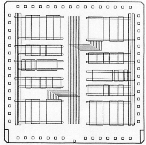
A standard signal bus structure may be integrated into the standard-cell-based chip layout if a number of cells must share the same input and/or output signals. Figure 3 depicts a simplified symbolic representation of a case in which a signal bus has been placed between standard cell rows.Since the chip in this case is made up of two blocks, power and ground must be routed from both sides of the layout field. Standard-cell based designs can contain many of these macro-blocks, each of which corresponds to a different unit of the system architecture, such as an ALU, control logic, and so on.


Figure-3: Simplified floorplan consisting of two separate blocks and a common signal bus.

The most difficult task is to position individual cells into rows and interconnect them in a way that meets stringent design goals in circuit speed, chip area, and power consumption after chip logic design is completed using standard cells from the library. To achieve these goals, several advanced CAD tools for place-and-route have been created and used.Circuit models with interconnect parasitics can also be extracted from the chip layout and used for timing simulation and analysis to define timing critical paths. To meet the timing criteria for critical paths, proper gate sizing is frequently used.Standard-cells-based design is used to implement complex control logic modules in many VLSI chips, such as microprocessors and digital signal processing chips. Some fully customised chips can also be built entirely out of standard cells.

Finally, Fig. 4 depicts the complex mask layout of a standard-cell-based chip with a continuous single block of cell rows and three memory banks on one side. The separations between neighbouring rows within the cell block are determined by the number of wires in the routing channel between the cell rows.If the routing channel can reach a high interconnect density, the standard cell rows can be positioned closer together, resulting in a smaller chip region. The availability of dedicated memory blocks also decreases the amount of space required, as memory elements created with standard cells will take up more space.


Figure-4: Mask layout of a standard-cell-based chip with a single block of cells and three memory banks.


Comments

Popular posts from this blog

Concepts of Regularity, Modularity and Locality

 By splitting the large structure into many sub-modules, the hierarchical design approach eliminates design complexity. To make the process easier, other design principles and approaches are usually needed. Regularity ensures that a large system's hierarchical decomposition can produce as many simple and identical blocks as possible.The design of array structures made up of similar cells, such as a parallel multiplication array, is a good example of regularity. Regularity can be seen at all levels of abstraction: uniformly sized transistors simplify the design at the transistor stage. Identical gate structures can be used at the logic level, and so on.A 2-1 MUX (multiplexer), a D-type edge-triggered flip flop, and a one-bit full adder are shown in Figure 7 as standard circuit-level designs. All of these circuits were created solely with inverters and tri-state buffers. This theory can be used to create a variety of different functions if the designer has a limited library of well-d...

Gate Array Design

The gate array (GA) comes after the FPGA because of the quick prototyping capability. As user programming is used to implement the design of the FPGA chip, metal mask design and processing is used to implement the design of the gate array. A two-step manufacturing process is needed for gate array implementation: The first phase, which uses generic (standard) masks, leaves each GA chip with an array of uncommitted transistors. These uncommitted chips can be saved for later customization after the metal interconnects between the array's transistors are defined (Fig. 1). Since the patterning of metallic interconnects is done at the end of the chip fabrication, the turn-around time can be still short, a few days to a few weeks. Figure 2 depicts a gate array chip's corner, which includes bonding pads on the left and bottom sides, diodes for I/O protection, nMOS and pMOS transistors for chip output driver circuits in the neighbouring areas of bonding pads, arrays of nMOS and pMOS tra...

Design Hierarchy

  Design Hierarchy The hierarchy, or 'divide and conquer' strategy, entails breaking down a subsystem into sub-modules and then repeating the process on the sub-modules until the smaller parts' complexity is manageable. This method is similar to how large programmes are broken down into smaller and smaller parts before simple subroutines with well-defined functions and interfaces can be written in software. The architecture of a VLSI chip can be expressed in three domains, as we've seen.As a result, each domain's hierarchy structure can be represented separately. However, it is important for design simplicity that the hierarchies in different domains can be easily mapped into one another. Figure 1 demonstrates the structural decomposition of a CMOS four-bit adder into its components as an example of structural hierarchy. Decomposing the adder into one-bit adders, separate carry and sum circuits, and finally individual logic gates is possible.The design of a simple c...