The gate array (GA) comes after the FPGA because of the quick prototyping capability. As user programming is used to implement the design of the FPGA chip, metal mask design and processing is used to implement the design of the gate array. A two-step manufacturing process is needed for gate array implementation: The first phase, which uses generic (standard) masks, leaves each GA chip with an array of uncommitted transistors. These uncommitted chips can be saved for later customization after the metal interconnects between the array's transistors are defined (Fig. 1). Since the patterning of metallic interconnects is done at the end of the chip fabrication, the turn-around time can be still short, a few days to a few weeks. Figure 2 depicts a gate array chip's corner, which includes bonding pads on the left and bottom sides, diodes for I/O protection, nMOS and pMOS transistors for chip output driver circuits in the neighbouring areas of bonding pads, arrays of nMOS and pMOS transistors, underpass wire segments, power and ground buses along with contact windows.
Figure-1: Basic processing steps required for gate array implementation.
Figure-2: A corner of a typical gate array chip.
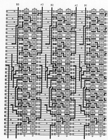
Figure 3 shows a magnified portion of the internal array with a metal mask template to realise a complex logic design (metal lines outlined in dark). As shown in Figs. 2 and 3, typical gate array platforms provide dedicated areas, called channels, for intercell routing between rows or columns of MOS transistors.And when only one metal layer is used, the availability of these routing channels simplifies interconnections. The interconnection patterns for implementing simple logic gates can be saved in a library, which can then be used to configure rows of uncommitted transistors based on the netlist.While most gate array platforms only have rows of uncommitted transistors separated by routing channels, others have dedicated memory (RAM) arrays to allow for higher density when memory functions are needed. The layout views of conventional gate array and a gate array platform with two dedicated memory banks are shown in Figure 4.
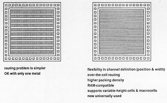
Routing can be done over the active cell areas using several interconnect layers, allowing the routing channels to be eliminated, as in Sea-of-Gates (SOG) chips. Uncommitted nMOS and pMOS transistors occupy the entire chip surface here.Neighboring transistors can be customised using a metal mask to form basic logic gates, much as in the gate array case. However, some of the uncommitted transistors must be sacrificed for intercell routing. This method provides more interconnection flexibility and, in most cases, higher density.Figure 5 depicts the basic platform of a SOG chip. A brief comparison of the channelled (GA) and channelless (SOG) approaches is shown in Figure 6.
Figure-3: Metal mask design to realize a complex logic function on a channeled GA platform
Figure-4 Layout views of a conventional GA chip and a gate array with two memory banks.
Figure-5: The platform of a Sea-of-Gates (SOG) chip.
Figure-6: Comparison between the channeled (GA) vs. the channelless (SOG) approaches.


Comments
Post a Comment