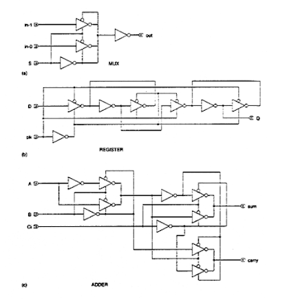
By splitting the large structure into many sub-modules, the hierarchical design approach eliminates design complexity. To make the process easier, other design principles and approaches are usually needed. Regularity ensures that a large system's hierarchical decomposition can produce as many simple and identical blocks as possible.The design of array structures made up of similar cells, such as a parallel multiplication array, is a good example of regularity. Regularity can be seen at all levels of abstraction: uniformly sized transistors simplify the design at the transistor stage. Identical gate structures can be used at the logic level, and so on.A 2-1 MUX (multiplexer), a D-type edge-triggered flip flop, and a one-bit full adder are shown in Figure 7 as standard circuit-level designs. All of these circuits were created solely with inverters and tri-state buffers. This theory can be used to create a variety of different functions if the designer has a limited library of well-defined and well-characterized basic building blocks. Regularity usually reduces the number of different modules that need to be designed and verified, at all levels of abstraction.
Figure 7: Regular design of a 2-1 MUX, a DFF and an adder, using inverters and tri-state buffers.The different functional blocks that make up the larger structure must have well-defined functions and interfaces, which is referred to as modularity in design. Since there is no doubt about the purpose and signal interface of these blocks, modularity allows each block or module to be constructed quite separately from the others. At the end of the design process, all of the blocks can be easily combined to shape the large structure. The principle of modularity allows the design process to be parallelized. It also enables the use of common modules in a variety of designs, thanks to the well-defined functionality and signal interface, which enables plug-and-play design.
We effectively ensure that the internals of each module become unimportant to the exterior modules by specifying well-characterized interfaces for each module in the framework. Internal specifics are left at the discretion of the local authorities. Locality also means that links are often made between adjacent modules, avoiding long-distance connections to the greatest extent possible. This final point is critical for preventing lengthy interconnect delays. Time-critical operations should be carried out locally, without the use of remote modules or signals. In large system architectures, the replication of certain logic may be sufficient to solve this issue.

Comments
Post a Comment