Design Hierarchy
The hierarchy, or 'divide and conquer' strategy, entails breaking down a subsystem into sub-modules and then repeating the process on the sub-modules until the smaller parts' complexity is manageable. This method is similar to how large programmes are broken down into smaller and smaller parts before simple subroutines with well-defined functions and interfaces can be written in software. The architecture of a VLSI chip can be expressed in three domains, as we've seen.As a result, each domain's hierarchy structure can be represented separately. However, it is important for design simplicity that the hierarchies in different domains can be easily mapped into one another.
Figure 1 demonstrates the structural decomposition of a CMOS four-bit adder into its components as an example of structural hierarchy. Decomposing the adder into one-bit adders, separate carry and sum circuits, and finally individual logic gates is possible.The design of a simple circuit understanding a well-defined Boolean function is much easier to manage at this lower level of the hierarchy than it is at the higher levels.
Partitioning a complex device into its different functional blocks would provide useful guidelines for the actual realisation of these blocks on chip in the physical domain. To create a useful floorplan, the approximate shape and size (area) of each sub-module must obviously be estimated. Figure 2 shows a basic floorplan generated by hierarchical decomposition of a four-bit adder in the physical description (geometrical layout) domain. This physical view shows the adder's external geometry, input and output pin positions, and how pin locations enable certain signals (in this case, carry signals) to be moved from one sub-block to the next without the use of external routing. At lower levels of the physical hierarchy, the internal mask

- Figure-1: Structural decomposition of a four-bit adder circuit, showing the hierarchy down to gate level.Figure-2: Hierarchical decomposition of a four-bit adder in physical (geometrical) description domain.

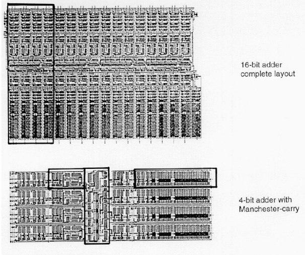

- Figure- 3: Layout of a 16-bit adder, and the components (sub-blocks) of its physical hierarchy.
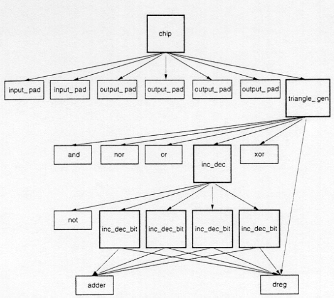
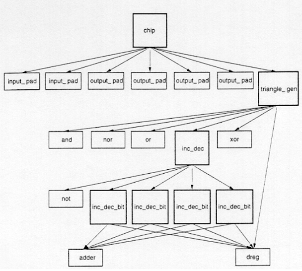 Figure-4: The structural hierarchy of a triangle generator chipFigure- 5: Physical layout of the triangle generator chip.
- layout of each adder cell defines the locations and the connections of each transistor and wire. Figure 3 shows the full-custom layout of a 16-bit dynamic CMOS adder, and the sub-modules that describe the lower levels of its physical hierarchy. Here, the 16-bit adder consists of a cascade connection of four 4-bit adders, and each 4-bit adder can again be decomposed into its functional blocks such as the Manchester chain, carry/propagate circuits and the output buffers. Finally, Fig. 4 and Fig. 5 show the structural hierarchy and the physical layout of a simple triangle generator chip, respectively. Note that there is a corresponding physical description for every module in the structural hierarchy, i.e., the components of the physical view closely match this structural view.


Comments
Post a Comment