For chip implementation of specified algorithms or logic functions, a variety of design styles can be considered. Each design style has its own advantages and disadvantages, so designers must make an informed decision in order to provide functionality at a low cost.
Field Programmable Gate Array (FPGA)
Users may order fully fabricated FPGA chips with thousands of logic gates or even more, as well as programmable interconnects, for custom hardware programming to achieve desired functionality. This design style allows for fast prototyping as well as cost-effective chip design, which is particularly useful for low-volume applications. I/O buffers, an array of configurable logic blocks (CLBs), and programmable interconnect structures make up a typical field programmable gate array (FPGA) chip. Programming of RAM cells whose output terminals are attached to the gates of MOS pass transistors is used to programme the interconnects.Figure 1 depicts the general architecture of an XILINX FPGA. Figure 2 shows a more detailed view of the locations of switch matrices used for interconnect routing.
Figure 3 depicts a basic CLB (model XC2000 from XILINX). Four signal input terminals (A, B, C, and D), a clock signal terminal, user-programmable multiplexers, an SR-latch, and a look-up table make up the system (LUT). The LUT is a digital memory that stores the Boolean function's truth table. As a result, it can produce any four-variable function or any two-variable function. The control terminals of multiplexers are not shown explicitly in Fig.3.
The CLB is set up in such a way that its array can be programmed to perform a variety of logic functions. To map complex functions, more sophisticated CLBs have been added. An FPGA chip's typical design flow begins with a behavioural summary of its features written in a hardware description language like VHDL.The synthesised architecture is then divided into circuits or logic cells using technology mapping (or partitioning). The chip design is fully defined in terms of available logic cells at this stage. Following that, the placement and routing stage assigns individual logic cells to FPGA sites (CLBs) and establishes cell routing patterns based on the netlist.
After routing is complete, the design's on-chip performance can be simulated and tested before the design is downloaded for FPGA programming. The chip's programming is true for as long as it is turned on, or until new programming is completed. In most cases, maximum utilisation of the FPGA chip region is not possible; as a result, several cell sites can go unutilized.
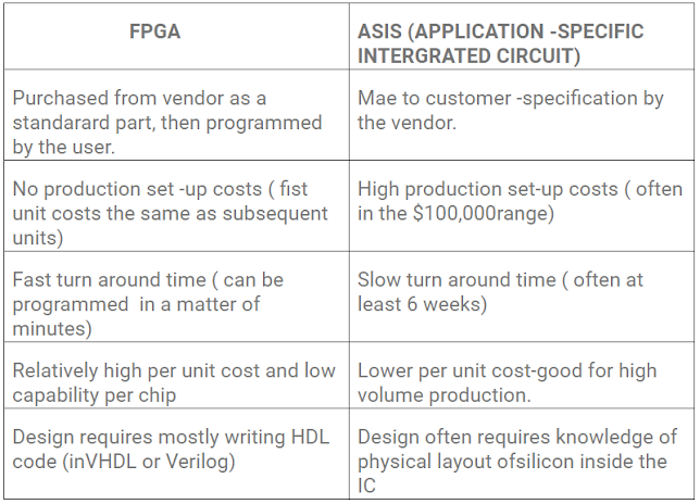
The most significant benefit of FPGA-based design is the extremely short time taken from the start of the design process to the availability of a working chip. Since the FPGA chip does not need any physical manufacturing, a functional sample can be obtained almost as soon as the concept is mapped into a specific technology. FPGA chips are typically more higher than other realisation options (such as gate array or standard cells) for the same design, but they are a very useful choice for small-volume ASIC chip development and quick prototyping, FPGA offers a very valuable option.


Comments
Post a Comment